
Schematic Design Of D-Latch and D-Flip Flop
D-LATCH
Latch is an electronic device that can be used to store one bit of information. The D latch is used to capture, or 'latch' the logic level present on the Data line when the clock input is high. If the data on the D line changes state while the clock pulse is high, then the output, Q, follows the input, D. When the CLK input falls to logic 0, the last state of the D input is trapped and held in the latch.
Timing diagram:
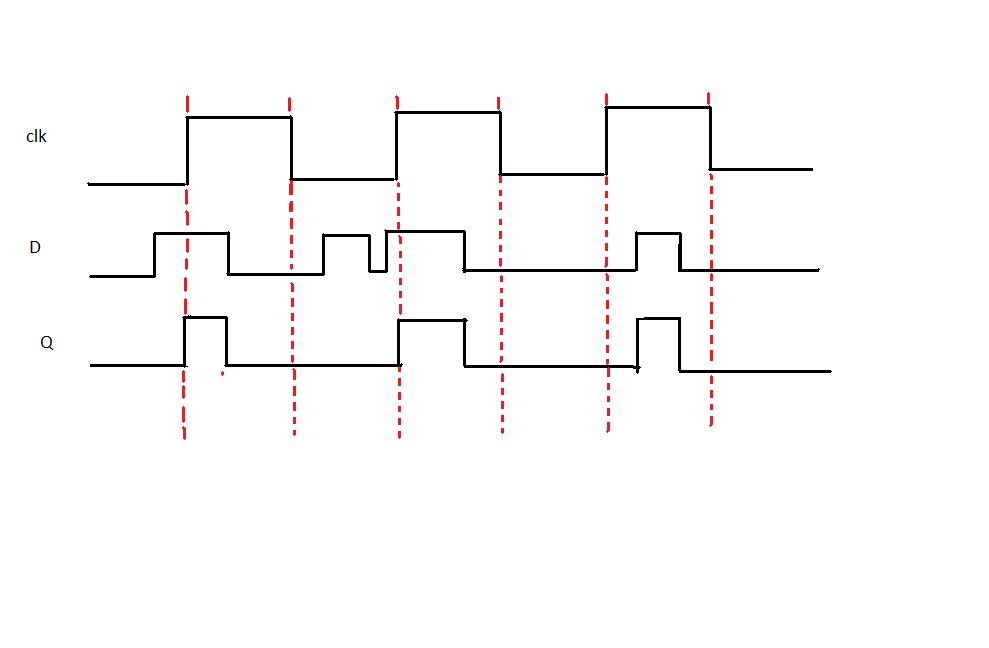
From the timing diagram, the output Q's waveform resembles that of input D's waveform when the clock is high, whereas when the clock is low Q retains the previous value of D (the value before clock dropped down to 0).
D FLIP FLOP
The working of D flip flop is similar to the D latch except that the output of D Flip Flop takes the state of the D input at the moment of a positive edge at the clock pin (or negative edge if the clock input is active low) and delays it by one clock cycle. That's why, it is commonly known as a delay flip flop. The D Flip-Flop can be interpreted as a delay line or zero order hold. The advantage of the D flip-flop over the D-type "transparent latch" is that the signal on the D input pin is captured the moment the flip-flop is clocked, and subsequent changes on the D input will be ignored until the next clock event.
Timing diagram:
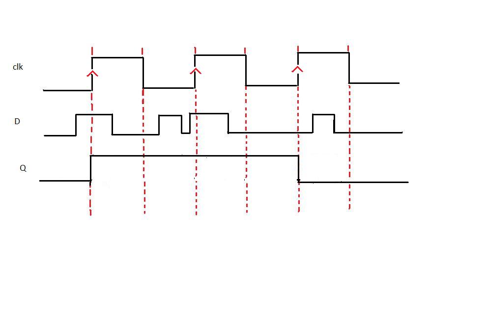
From the timing diagram, the output Q changes only at the positive edge. At each positive edge the output Q becomes equal to the input D at that instant and this value of Q is held until the next positive edge.
Characteristics and applications of D latch and D Flip Flop:
- D-latch is a level Triggering device while D Flip Flop is an Edge triggering device.
- The disadvantage of the D FF is its circuit size, which is about twice as large as that of a D latch. That's why, delay and power consumption in Flip flop is more as compared to D latch.
- Latches are used as temporary buffers whereas flip flops are used as registers.
- Flip flop can be considered as a basic memory cell because it stores the value on the data line with the advantage of the output being synchronized to a clock.
- Many logic synthesis tools use only D flip flop or D latch.
- FPGA contains edge triggered flip flops.
- D flip flops are also used in finite state machines.
Edge Triggering vs. Level Clocking
- When a circuit is edge triggered the output can change only on the rising or falling edge of the clock. But in the case of level-clocked, the output can change when the clock is high (or low).
- In edge triggering output can change only at one instant during the clock cycle; with level clocking output can change during an entire half cycle of the clock.
Working of the latch when clock is 1.
When clock is 1 the pass transistor in red is on (the input to the gate of nmos is 1 and to the gate of pmos is 0) therefore the output is D. As D changes the output changes accordingly. The two inverters act as a buffer.
Working of the latch when clock is 0.
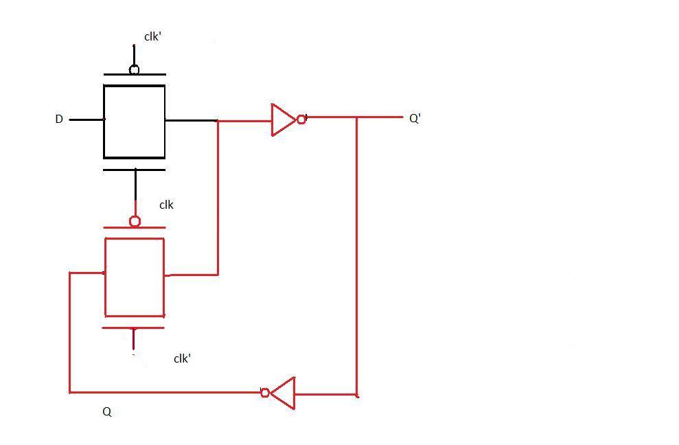
When clock is 0 the pass transistor in red is on and the one connected to the input D is off thus any changes in D does not affect the circuit. If we observe the transistor in red is connected to the buffer at the output which loops back to its input thus the same value occurs at Q' again and again till this pass transistor is on.
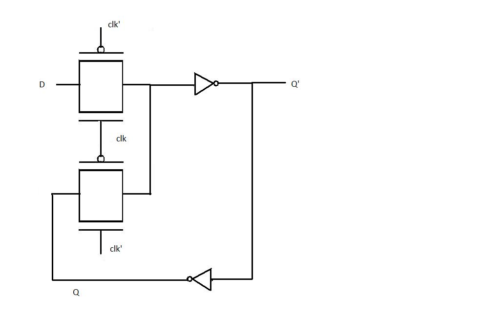
POSITIVE EDGE TRIGGERED FLIP FLOP
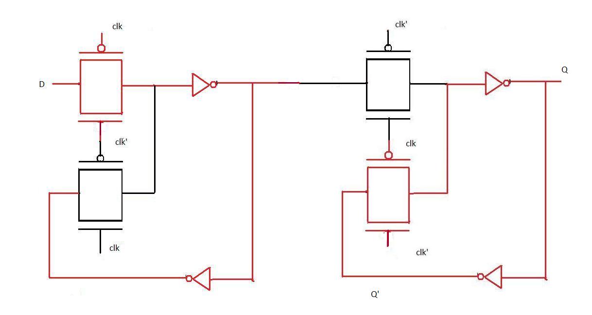
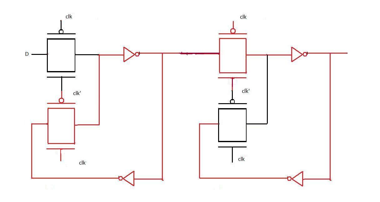
From the introduction it is clear that for a positive edge triggered flip flop the changes in output occurs at the transition level. This is done by configuring two D latches in master slave configuration.A master slave D flip-flop is created by connecting two gated D latches in series, and inverting the clock input to one of them. It is called master slave because the second latch in the series only changes in response to a change in the first (master) latch. To understand the transistor level design of positive edge triggered flip flop study the two diagrams below
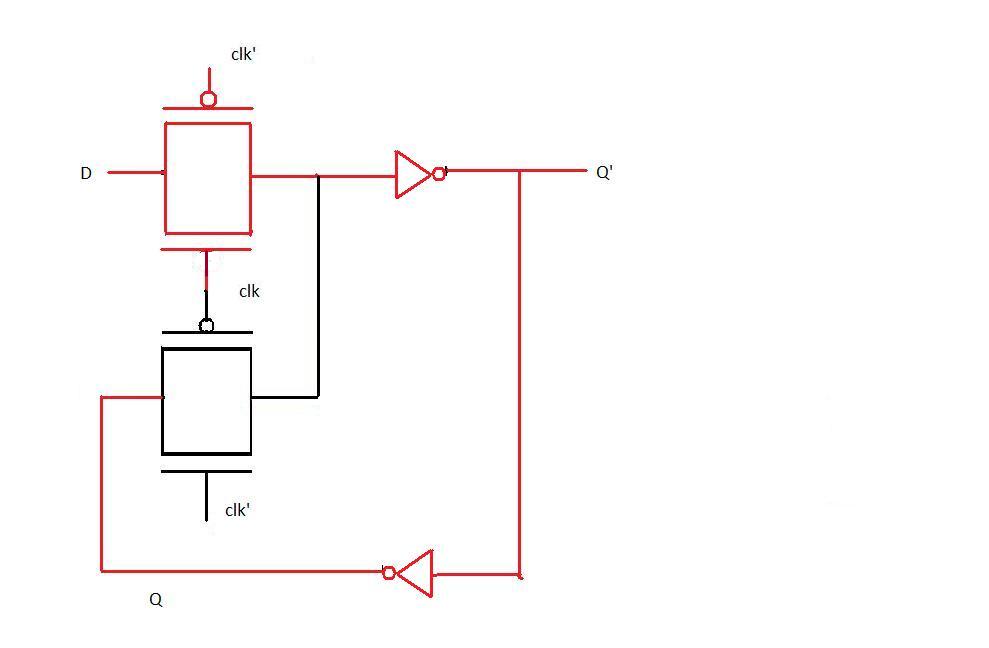
Positive edge triggered flip flop when clock=0
As evident from the figure when clk is 0 the input D passes through the first level of pass transistor logic and held there because the second level does not pass on the value of D
Positive edge triggered flip flop when clock=1
When the clock input becomes 1, D(at that instant) is transferred to the output. Thereafter output Q does not change when D changes because D is not passed through the first level of pass transistor logic (as seen in the diagram). Now when the clock changes back to 0, Q still remains unaffected by the changes in D because it is now hindered by the second level of pass transistor. Thus we observe that Q remains unchanged for the entire clock cycle and changes only at the positive edge. Hence the above transistor level diagram implements positive edge triggered flip flop.
APPLICATION AND ADVANTAGES OF D- FLIP FLOP
D flip flop can be considered as a basic memory cell because it stores the value on the data line with the advantage of the output being synchronised to a clock. D flip flops form the basis of shift registers that are used in many electronic devices. Many logic synthesis tools use only D flip flop or D latch. FPGA contains edge triggered flip flops. D flip flops are also used in finite state machines.