
Design Of D-Flip Flop Using Verilog
A D Flip-Flop is a fundamental sequential circuit element used to store and transfer data in digital systems. Unlike combinational circuits, sequential circuits use memory elements (like flip-flops) to store state information. The D Flip-Flop, also known as a data or delay flip-flop, captures the value of the input (D) at a specific clock edge and holds it until the next clock event.
Working Principle
- Positive Edge D Flip-Flop: The output Q takes the value of D at the rising (positive) edge of the clock (CLK).
- Negative Edge D Flip-Flop: The output Q takes the value of D at the falling (negative) edge of the clock.
Truth Table
| CLK Edge | D | Q (Next) |
|---|---|---|
| Rising/Falling | 0 | 0 |
| Rising/Falling | 1 | 1 |
Timing Diagram
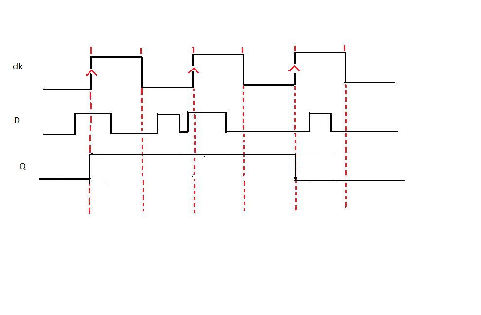
The output Q changes only at the specified clock edge, matching the value of D at that instant.
Verilog Implementation
A D Flip-Flop can be described in Verilog using an always block triggered by the clock edge:
verilog
          module d_flip_flop (
              input D,
              input CLK,
              output reg Q
          );
              always @(posedge CLK) // Use negedge CLK for negative edge
              begin
                  Q <= D; // Non-blocking assignment for sequential logic
              end
          endmodule
- The module defines inputs D and CLK, and output Q.
- The
alwaysblock updates Q at the clock edge. - Non-blocking assignment (
<=) ensures correct sequential behavior.
Testbench and Simulation
To verify the D Flip-Flop, a testbench is used to generate input waveforms and observe the output:
- Declare D and CLK as registers, Q as a wire.
- Instantiate the D Flip-Flop module.
- Define input and clock waveforms.
- Observe the output Q in response to changes in D and CLK.
Experiment Simulation Steps
- The simulation page divides the Verilog module and testbench into colored code blocks.
- Drag and drop the code blocks to arrange them in the correct order.
- Complete the code blocks by entering module names, selecting inputs/outputs, and filling in the always block.
- Click Validate to check your code and view the output table and waveforms.
Key Points
- Use non-blocking assignment (
<=) for sequential logic. - Select the correct clock edge (
posedgeornegedge) based on the flip-flop type. - Ensure module and testbench names follow Verilog naming conventions.
- Observe how Q responds to D and CLK in the simulation.